The 3 Tools to Reverse a Simple PCB
Published by Fast PCB Studio on
The 3 Tools to Reverse a Simple PCB
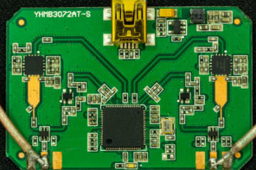
Circuit boards Reverse Engineering, also known as PCB cloning. Reversing a complex board needs to be familiar with the circuit design software, also required to have the hardware circuit background to resolve the possible problems whenever the reversing works encounter in the electromagnetic compatibility, electromagnetic interference issues. The reverse engineers must have a certain ability to resolve these issues.
For PCB reverse engineering, at present, as long as the copy software can directly open and save the PROTEL PCB file, all placed in the element properties fully supporting PROTEL format, including the placement function, it’s possible to copy any type of boards, theoretically.
Today, we would like to share you the 3 common tools on reversing a simple PCB, so you may do it yourself by following tips:
1. Suitable Scanner
The accuracy of the copy board, depending on the two procedures, one is the accuracy of the software, one is the original image accuracy. The software used for precision 32-bit floating-point representation can be said that there is no accuracy limit, so the most important thing is depending on the accuracy of the original scan image. For example, if taking a 1-megapixel photo washable 5-inch photo, but if it’s expected to wash into a 20-inch photo it simply can not see clearly. Similarly, for PCB scanning for high precision circuit board, it must choose a higher DPI (Dot per Inch) in the scanning. In other words, the distance between every two points on the scanned image is 1000 / DPI in mil. If the DPI is 400, the distance between two points on the image is 1000/400 = 2.5 mil, that is The accuracy at this moment is 2.5mil. The normal high intensive induction PCB line width/gap will be over 4 mil.
PCB Reverse Engineering Services
Simply done your PCB reverse engineering project @Chinapcbcopy.com from US$150.00/board.
We will deilver the engineering file into:
- PCB Gerber File
- BOM List
- Schematic Diagram
*PCB bare board will be delayered during the procedure and the sample PCB will no longer be able to reuse.
2. PCB Reverse Engineering software
Software copy board is mainly depends on whether the function is complete, it is best to copy all the work can be done in the software, so that efficiency is high, including the placement of components to support PROTEL99SE as the 99SE component library is very powerful, and can be downloaded from the Internet directly. The era of hand-made components is over because many components, like BGP components, have sealed with over hundreds of components, and it would be too costly to build manually.
For the stability of the circuits, the design of the circuit generally have a large copper area to connect with power line or ground line, this can reduce the circuit noise and interference. So it involves the issue of network copper laying. For complex circuit boards, there are a lot of copper laying to connect while there are many to be isolated. If the problem is not solved properly, copper laying can not be added correctly, so here must be defining the network to pave the area for copper ( e.g. “same network connection, different network isolation”).
3. Layer Grinding
For multi-layer PCB reverse engineering, the middle layer can not be scanned directly. To copy multi-layer board, it must be milled out, so the multi-layer PCB will be damaged anyhow after the reversing work.
The current common method is to use a fine grinding machine or hand grinding. Some PCBs require both methods to get into the mid-layers. The procedure requires very experienced technicians to operate as some samples are very fragile and the copper layer could be easily damaged during the process.