Fast PCB Studio
PCB Reverse Engineering Services
PCB Reverse Engineering Services
- PCB Gerber File
- BOM List
- Schematic Diagram
*PCB bare board will be delayered during the procedure and the sample PCB will no longer be able to reuse.
Why PCB Reverse Engineering
PCB hardware reverse engineering enables PCB re-production possibility when the production related PCB engineering files are no longer exist. The reversed engineering files will enable the re-production of the PCB hardware.
Electronics engineers & product developers are also able to learn useful design ideas from exisitng boards, therefore use the idea on their own designs.
Info Required for Quotation
For a proper quotation for your PCB reverse engineering project, we will need the information from you as below:
1. Layer of PCB - How many layers of your PCB sample
* E.g. 4 or 6 Layer PCB.
If you cannot provide the info, please share the info regarding the function of the PCB board, and we will reasoning the layers as per our experiences.
2. Dimensions of the PCB board
* E.g. 100mm*110mm
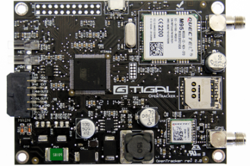
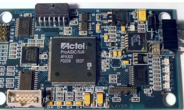
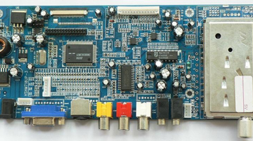
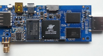
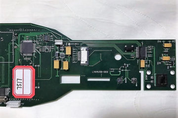
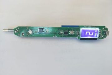
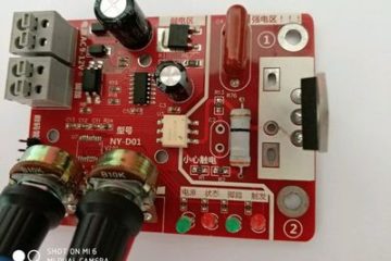
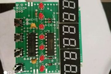
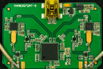
3. Top & Bottom pictures clearly showing all the components on board
* A lot of PCB boards are assembled with programmable IC / ICs to make the board. You will need to consider IC unlock for the programmable ICs if you don’t have
software solutions if you plan to copy a PCB from sample board. Clearly showing the ICs on board and check with us the IC model numbers, if you would like to use
the PCB reverse engineering files for re-production. However, please be advised that only embedded programs burnt into programmable ICs are potentially unlocked.
Other software that are not stored in programmable ICs will not copyable through IC Unlock technology.
Service Details
1. Capability
- 1-28 layer PCBs (Industrial, consumer, medical, computer boards & etc.)
2. Service content
- Physical PCB reverse engineer to PCB files / BOM / Schematics
- Design software – Protel99 SE
- Work output & files delivery – PCB file in Protel & CAM / BOM list / Schematics in Protel & PDF
3. Pricing
Service charge from USD150. Price guideline as below for the references:
- 100*100mm 2-4 layer PCB: approx. USD400 – 1000
- 100*100mm 6-8 layer PCB: approx. USD700 – 1800
- Higher layers price can be vary depending on the complexity of the design
*Price will be quoted case by case per PCB size / amount of pads and vias / complexity of traces / via types / substrate materials & etc.
**We will need PCB dimension + Clear PCB top & bottom pictures + PCB layer info for a formal quotation
4. Service Flow
- Shipping samples to FAST PCB STUDIO
- 50% initial payment to start the project
- PCB RE work starts after sample & initial payment receival
- RE work completion, sending proof of work (PCB PDF Schematics / Gerber screenshot)
- Final 50% payment receival
- Submit all the engineering files
- Project closed
PCB Reverse Engineering Q&A
- Q1: How much to Copy a PCB?
- A1: PCB Reverse Engineering price is related to multiple factors. Generally, PCB layer affects the price the most. Higher the layer is, more expensive the PCB copy would be.
- Q2: How to choose a PCB Reverse Engineering services provider?
- A2: The service provider needs to be very experienced on PCB Copy to zero the possible errors for the final engineering files for production. Fast PCB Studio is able to transfer your the PCB module sample to the Gerber file for PCB production, the other universal PCB file format, as well as the BOM list and the schematic diagram of the PCB. We have the testing team to check circuits we captured from the sample module, and make sure there is no difference between the physical PCB module and PCB Gerber we are providing.
- Q3: What I can receive once the PCB Reverse Engineering work done?
- A3: We provide our customers PCB Gerber file, BOM list, and PCB Schematic Diagram. Customer is able to make the PCB module through the files.
- Q4: Will Fast PCB Studio resell the customers’ files?
- A4: All the PCB samples from customer & the files customer paid for are highly confidential between Fast PCB Studio & the customers. We have been cooperating with a lot of our customers for so many years, and we have been obeying the business integrity and protecting every piece of our customers’ information.
- Q5: Why the price of PCB Reverse Engineering Service prices are very different between the service providers?
- A5: The accuracy of circuits on line width, space, holes size & etc. can be different between the service providers. Some are not so experienced on PCB Copy, so customer may have to re-work many time with they, and re-make PCB module many time to achieve the expected result. With 10+ years experiences on various projects covering Consumer / Automotive / Medical / Military / Industrial / Telecom appliances, Fast PCB Studio is capable to handle those simple multi-layer PCB on zero failure rate.
- Q6: How do you ensure the PCB copied 100% correct?
- A6: Fast PCB studio has its proven PCB copy procedures to ensure the accuracy of the graphs captured. After the files are generated, there will be the experienced engineers to check all the files.
- Q7: Does PCB Reverse Engineering Services require to disassemble the PCB components? Is PCB sample re-usable?
- A7: It depends on the complexity of the PCB. If it’s 1-2 layer PCB, it’s possible to Copy without disassemble the PCB Module. However, to disassemble PCB sample is highly recommended, as the PCB Copy is able to be completed without error by doing this. The PCB sample from the customer may be re-usable if it’s simple 1 or 2 layer PCB module.
- Q8: Why there is a project assessment before we accepting your PCB Reverse Engineering Service request?
- A8: There are some factors may affect PCB Copy work. The function of the PCB module, Special IC coding type, special IC availability & etc. may fail a PCB Copy work. Thus, our engineers will assess the project before we accept it.
PCB Cloning Steps
From PCB Cloning to PCBA Re-production
1. PCB reverse engineering & IC Unlock
We copy the design of the PCBA your need, and extract the machine code of IC program for the new IC duplication. We will send you 2 duplicated IC for your testing as this stage. Shipment cost of new IC samples are not included in service charge.
a. Shipping samples to FAST PCB STUDIO
b. 50% initial payment to start the project (PCB RE or IC Unlock or both)
c. PCB RE and/or IC unlock work starts after sample & initial payment receival
d. Unlock and/or RE work completion, sending proof of work (IC samples and/or PCB PDF Schematics / Gerber screenshot)
e. Final 50% payment receival
f. Submit all the engineering files
g. Close the project of IC unlock and/or PCB RE
2. PCBA sampling quotation & Mass production quotation
We will quote the PCBA for you once we obtain all the engineering files for re-production. The quotation for sampling and mass production will be available at this stage.
3. Prototype copied PCB & Multiple Testing
The same PCBA samples will be built for testing & debug. We will send you the sample boards for your approval before MP.
a. Quote for Prototype & Mass production
b. 100% payment before PCBA Prototype
c. Prototype complete. Testing & Debug, BOM / PCB file correction
d. Sending prototypes back to customer for testing
e. Approval of prototypes received from customer
4. PCBA Production
We will manufacture then delivery the MP of PCBA to your address.
a.100% payment receival before mass production
b.PCBA component sourcing + Assembly + Testing
c.PCBA MP ready to ship out
Why Us
Fast PCB Studio is one of the Leading PCB Copy & IC Unlock service provider in Dongguan, China. We are dedicated to provide our clients the very reliable & cost effective Full solution for Electronic Reverse Engineering & Production.
(1) Under normal circumstances, the single-layer and double-layer board take upto 3-5 working days, the 4-6 layer board takes upto 7 to 12 workding days, and the 10+ layer board takes upto 12 to 15 working days. The multilayer board depends on the complexity of the circuit board;
(2) We have strong R&D resources and strong R&D support team in Beijing and Shenzhen, and we have our own talent training tutorial from experienced PCB reverse engineered in Shenzhen, which ensures 100% accuracy of PCB copy board;
(3) “To create a win-win situation with customers” is always our principle for cooperation. Based on your specific requirements, we will provide the most reasonable quotes in very short time, and would help to evaluate the cases from your pictures or samples free of charge.
*We are capable to generate the documents in various format with additional charge. In gerneral, we use software Protel99/Se.
We not only focus on advanced technology, but also carry out quality management of the entire PCB production process, including excellent product design, high-quality materials, suitable equipment, mature production processes, skilled production personnel, and strict and meticulous inspection, storage, packaging and so on.
We have the strong networks for electronic products from reverse engineering to productions. Our partners empowered us to provide the full solutions for PCB copy, PCBdesign & Modification, prototype error fixing, IC decryption (As known as IC Unlock or IC Crack), IC procurement, high-precision board production with state of art SMT facilitise, PCB assembly testing (Including BGA X-ray testing) and turnkey services. We could also provide design for products according to customer requirements, including the re-design / modification for the development of the existing product on function improvement and technical optimization in some fields.
We support our customers the after-sell services for all the designs and the productions from us.
Disclaimer: The use of our reverse engineering technologies is strictly limited within legal purposes, e.g. reproduce PCB artworks for old or obsolete printed circuit boards where the original is no longer available, PCB & Design tutorial or research and etc. Fast PCB Studio would not be responsible for any legal disputes for any inappropriate use of our technology on commercial competition, patent duplication or other prohibited use of reverse engineering technology by local laws.